Experiencing sudden micro-stutters mid-game, perceptible input lag upon moving a mouse, or unexplained throughput bottlenecks despite owning a flagship NVMe SSD rarely stems from weak individual components. Instead, these anomalies point to data bus congestion and synchronization drift across the motherboard's copper traces. Pairing a flagship CPU with a top-tier GPU achieves little if the underlying communication buses and signaling protocols are bottlenecked.
Computer hardware components communicate via high-frequency binary voltage pulses (0s and 1s) routed across multi-layer copper PCB traces known as System Buses. This architecture relies on three specialized pathways: the Address Bus (locating data), the Data Bus (transporting payloads), and the Control Bus (managing read/write arbitration). Components synchronize via a master Clock Cycle and request immediate CPU attention using hardware Interrupt Requests (IRQs).
Table of Contents
- 1. The Motherboard Nervous System: Address, Data & Control Buses
- 2. The System Metronome: Clock Cycles & Serpentine PCB Traces
- 3. Knocking vs. Direct Access: IRQ Interrupts & DMA Physics
- 4. Modern Highways: PCIe Lanes, DMI & Chipset Topologies
- 5. System Bus Technical Comparison Matrix
- 6. Applied Scenario: The 14ms Silicon Journey of a Mouse Click
- 7. Frequently Asked Questions (FAQ)
Those serpentine zigzag copper traces on a motherboard are not aesthetic flair; they are precision delay lines ensuring high-frequency electrical pulses arrive within the exact same picosecond.
1. The Motherboard Nervous System: Address, Data & Control Buses
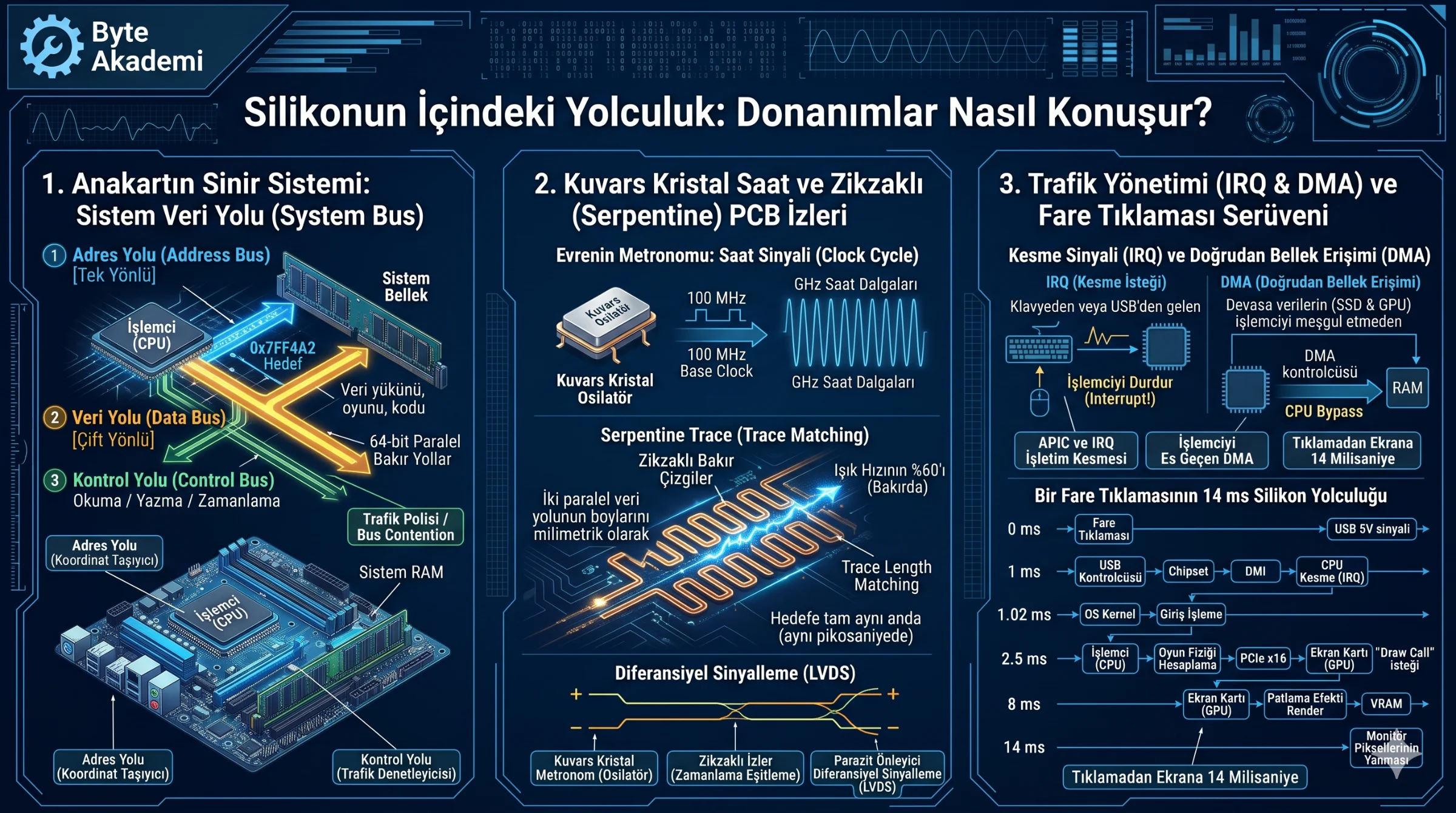
Beneath a motherboard's solder mask lie thousands of microscopic copper traces forming the System Bus, divided into three functional layers:
- Address Bus (Unidirectional): Carries physical memory coordinates from the CPU to RAM or peripherals. Its bit-width (e.g., 64-bit) defines the maximum addressable memory space.
- Data Bus (Bidirectional): Transports actual binary payloads (textures, instructions, variables) back and forth. A 64-bit data bus transfers 8 bytes simultaneously per clock cycle.
- Control Bus (Arbitration): Prevents bus contention by carrying timing, read/write, and acknowledgment signals so multiple devices do not corrupt shared lines.
  [TRI-BUS CPU-TO-MEMORY ARCHITECTURE]

  ┌─────────────┐  1. Address Bus (Unidirectional: Target Coordinates) ┌─────────────┐
  │             │ ---------------------------------------------------> │             │
  │     CPU     │  2. Data Bus (Bidirectional: 0 & 1 Binary Payloads)  │     RAM     │
  │ (Processor) │ <==================================================> │  (Memory)   │
  │             │  3. Control Bus (Read/Write & Timing Arbitration)    │             │
  └─────────────┘ <--------------------------------------------------> └─────────────┘
2. The System Metronome: Clock Cycles & Serpentine PCB Traces
Synchronization across billions of transistors relies on a piezoelectric Quartz Crystal Oscillator generating a precise base clock (BCLK, typically 100 MHz), which internal PLL multipliers scale into gigahertz frequencies.
Because electrical signals propagate through copper at roughly 60% the speed of light (~180,000 km/s), even a 1-millimeter trace length mismatch at GHz speeds causes clock skew and bit corruption. Engineers deliberately route shorter traces in wavy serpentine patterns to match physical lengths to the picosecond, while employing Low-Voltage Differential Signaling (LVDS) across paired wires to cancel electromagnetic interference.
3. Knocking vs. Direct Access: IRQ Interrupts & DMA Physics
Instead of wasting CPU cycles continuously polling idle devices, hardware utilizes two streamlined mechanisms:
- IRQ (Interrupt Request): When a key is pressed or a network packet arrives, peripheral controllers trigger an electrical interrupt via the APIC, prompting the CPU to pause its current thread, save register states, service the event, and resume.
- DMA (Direct Memory Access): High-throughput devices like NVMe SSDs and GPUs bypass CPU execution cores entirely via a DMA Controller, streaming gigabytes of textures directly into system RAM without stalling processor threads.
4. Modern Highways: PCIe Lanes, DMI & Chipset Topologies
Legacy Northbridge logic now resides directly inside the CPU silicon die. Primary high-speed components—the GPU (PCIe x16) and primary NVMe SSD (PCIe x4)—connect directly to CPU PCIe lanes via full-duplex differential pairs. Meanwhile, USB controllers, audio codecs, Wi-Fi, and SATA drives route through the motherboard Chipset (Southbridge), sharing a single bottleneck uplink—the DMI (Direct Media Interface)—back to the processor.
5. System Bus Technical Comparison Matrix
| Interconnect / Protocol | Connected Endpoints | Theoretical Bandwidth | Topology | Typical Latency |
|---|---|---|---|---|
| CPU Ring Bus / Mesh | CPU Cores & L1/L2/L3 Caches | 1,000 - 3,000+ GB/s | On-die parallel mesh | 0.5 - 3 Nanoseconds |
| DDR5 Memory Bus | CPU IMC ↔ System RAM | 51.2 - 102.4 GB/s (Dual Channel) | 2x 64-bit Parallel Bus | 55 - 75 Nanoseconds |
| PCIe 5.0 x16 Link | CPU ↔ Discrete GPU | 64 GB/s (Unidirectional) / 128 GB/s | Point-to-point serial | ~100 - 200 Nanoseconds |
| PCIe 4.0 x4 NVMe | CPU ↔ Primary M.2 SSD | 7.88 GB/s (~7,500 MB/s real) | Full-duplex serial | 10 - 20 Microseconds |
| DMI 4.0 x8 Chipset | CPU ↔ Motherboard Chipset | 15.75 GB/s (Shared uplink) | Shared serial bridge | Variable (Traffic-bound) |
6. Applied Scenario: The 14ms Silicon Journey of a Mouse Click
  [STEP 1 - 0.00 ms] Mouse microswitch closes; differential 5V packet travels via USB cable.
  [STEP 2 - 1.00 ms] Motherboard USB controller receives packet and fires an IRQ over DMI to CPU.
  [STEP 3 - 1.02 ms] OS Kernel traps the interrupt and passes input coordinates to the game engine.
  [STEP 4 - 2.50 ms] CPU computes ballistics and issues Draw Calls over PCIe 5.0 x16 to the GPU.
  [STEP 5 - 8.00 ms] Thousands of GPU shader cores render the frame into high-speed GDDR VRAM.
  [STEP 6 - 14.0 ms] DisplayPort 2.1 streams frame bits to the monitor; pixels illuminate!
7. Frequently Asked Questions (FAQ)
Why are motherboard copper traces drawn in wavy zigzag patterns instead of straight lines?
At multi-gigahertz frequencies, parallel data lines must arrive within picoseconds of each other to avoid clock skew. Engineers route shorter traces in serpentine zigzags to match the exact physical length of longer neighboring traces.
Can populating multiple M.2 SSD slots reduce GPU PCIe bandwidth?
Yes. Consumer CPUs provide a fixed number of direct PCIe lanes (typically 20 to 28). Installing additional M.2 drives on certain motherboards splits the primary GPU slot from x16 down to x8 or routes secondary drives through the shared chipset DMI link.
Why did serial interfaces (PCIe, SATA) replace parallel ribbons (IDE, PCI)?
Parallel wires running side-by-side suffer severe electromagnetic crosstalk and signal skew at high clock speeds. Serial differential signaling eliminates cross-wire interference, enabling dramatically higher clock frequencies and throughput over fewer copper pins.